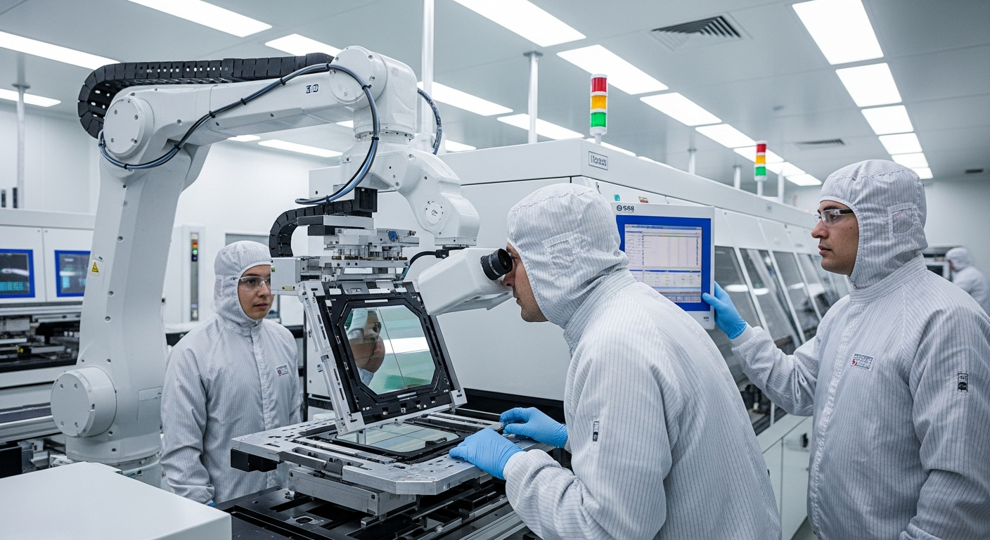
Understanding semiconductor manufacturing processes
Semiconductors are the foundational elements powering virtually every electronic device in the modern world. From the smartphones in our pockets to the vast data centers that underpin the internet, these tiny components, often no larger than a fingernail, enable the complex computational tasks that define our digital age. Understanding their intricate manufacturing processes offers insight into the technological advancements that continuously reshape our daily lives and drive global innovation.

The Foundation: Wafer Preparation and Circuit Design
The journey of a semiconductor begins with highly purified silicon, typically extracted from sand, which is then grown into large, single-crystal ingots. These ingots are meticulously sliced into thin wafers, polished to an atomic-level flatness, and prepared as the substrate for countless integrated circuits. Before any physical manufacturing begins, extensive design work is undertaken, leveraging sophisticated software tools to lay out the intricate patterns of transistors and interconnections that will form the desired circuits. This phase of engineering and development is crucial, as it defines the functionality and performance of the final digital devices, from simple logic gates to complex processors and memory units.
Patterning with Photolithography and Etching
One of the most critical stages in semiconductor manufacturing is photolithography, a process akin to photography. Here, a light-sensitive material called photoresist is applied to the wafer. A mask, containing the circuit pattern, is then used to expose specific areas of the photoresist to ultraviolet light. The exposed or unexposed areas are then removed, leaving behind a patterned layer. Following this, etching processes remove material from the wafer in the areas not protected by the remaining photoresist, effectively transferring the circuit pattern onto the silicon substrate. This precise patterning is repeated numerous times, layer by layer, to build up the complex three-dimensional structures of transistors and interconnects essential for modern computing hardware.
Building Layers: Deposition, Doping, and Interconnection
Once patterns are etched, various materials are deposited onto the wafer. Thin films of insulating oxides, conductive metals, and other semiconductor materials are added using techniques like chemical vapor deposition (CVD) or physical vapor deposition (PVD). Doping, another crucial step, involves introducing specific impurities into the silicon to alter its electrical conductivity, creating the n-type and p-type regions that form transistors. As more layers are built, metal interconnects, often made of copper, are fabricated to link the millions or billions of transistors together, forming the intricate networks that allow data to flow within a chip. This integration of diverse materials and processes is what enables the creation of highly sophisticated systems.
Ensuring Performance: Testing and Quality Control
Throughout the manufacturing process, and especially at the end, rigorous testing is conducted to ensure the functionality and reliability of the semiconductor devices. Each chip on the wafer undergoes electrical testing to verify that its circuits perform as designed. Defective chips are identified and marked. This meticulous quality control is vital because even a single faulty transistor can render an entire processor or memory chip unusable. The commitment to precision at every step highlights the advanced technology and innovation required to produce components that meet the demanding performance standards of today’s digital world.
Packaging and Final Integration for Connectivity
After testing, the wafers are cut into individual chips, known as dies. Each functional die is then carefully packaged. Packaging protects the delicate silicon chip from environmental damage and provides a means to connect it to other components on a printed circuit board. This involves attaching the die to a lead frame or substrate and encapsulating it. The package also provides the necessary electrical connections, or pins, that enable the chip to communicate with other devices and systems, facilitating connectivity within larger electronic assemblies. This final stage transforms the raw silicon into a usable component for a vast array of electronic devices, from consumer electronics to industrial computing systems.
The Future of Semiconductor Development
The semiconductor industry is characterized by continuous innovation and rapid development. Researchers and engineers are constantly pushing the boundaries of what is possible, exploring new materials, manufacturing techniques, and architectural designs. The drive for smaller, faster, and more energy-efficient processors and memory solutions fuels advancements in areas like artificial intelligence, high-performance computing, and advanced digital displays. This relentless pursuit of progress ensures that the technology sector will continue to deliver more powerful and integrated solutions, impacting everything from personal devices to global data networks and shaping the future of technology for years to come.
The manufacturing of semiconductors is a highly complex and capital-intensive endeavor, requiring a blend of advanced science, precision engineering, and innovative technology. From raw silicon to a fully functional integrated circuit, each step demands meticulous control and sophisticated processes. These tiny components are the unseen engines driving the digital revolution, enabling the vast array of electronic devices and systems that define modern life and continue to evolve at an astonishing pace.


